



Economy
India's Semiconductor Mission 2.0 Enters Landmark Phase With Rs 1.27 Lakh Crore Push
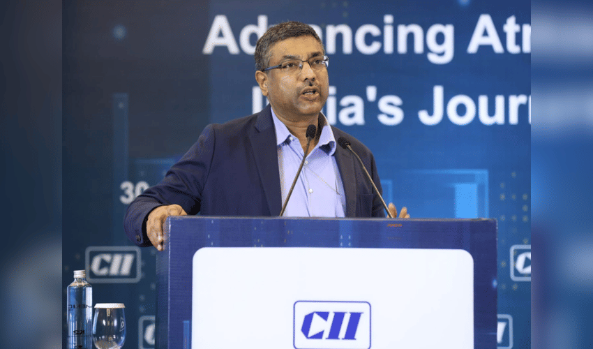

India's semiconductor industry is moving into a new phase of growth as the government officially launches the India Semiconductor Mission 2.0 (ISM 2.0) with a financial outlay of ₹1.27 lakh crore. Ministry of Electronics and Information Technology (MeitY) Secretary S Krishnan described 2026 as a “landmark year” for India’s chip manufacturing ambitions while speaking at the CII Conference on Advancing Atmanirbharta in Semiconductor Design and Manufacturing.
Krishnan said the latest phase of the semiconductor mission reflects India’s growing determination to build a self-reliant electronics ecosystem and reduce dependence on global supply chains. He added that the government’s semiconductor push is now moving beyond individual manufacturing units and towards developing a complete industry ecosystem. Highlighting the progress achieved under ISM 1.0, Krishnan said three semiconductor facilities inaugurated by Prime Minister Narendra Modi — including Micron’s semiconductor unit, Tata’s plant in Sanand, and the CG Power facility — have already entered commercial production. Two more semiconductor units are expected to become operational before the end of the year, while 12 additional projects approved under the India Semiconductor Mission are currently in various stages of development.
He also noted that India’s chip design ecosystem has gained momentum, with 15 out of the 24 companies approved under the Design Linked Incentive (DLI) scheme securing venture capital funding. The development, according to him, indicates increasing investor confidence in India’s semiconductor design capabilities. The Union Cabinet recently approved ISM 2.0 along with a separate mobile phone manufacturing programme, together involving an investment commitment of around ₹1.90 lakh crore. Krishnan said the decision came after detailed consultations with industry stakeholders and reflects the government’s long-term commitment to strengthening India’s electronics manufacturing sector.
Under ISM 2.0, the government will continue to focus on establishing semiconductor fabrication plants, Assembly, Testing, Marking and Packaging (ATMP) facilities, and Outsourced Semiconductor Assembly and Test (OSAT) units. Building on the three fabs currently being developed under ISM 1.0, India aims to add four to five more facilities, including a logic semiconductor fab, memory chip manufacturing unit, display facility, and multiple compound semiconductor plants.
Advanced packaging technology will also remain a major priority. According to Krishnan, eight advanced packaging units are already being developed under the first phase of the semiconductor mission, with three of them having started production. A major shift under ISM 2.0 will be the government’s broader ecosystem approach. Unlike the first phase, which focused mainly on manufacturing capacity, the new programme will also support industries involved in semiconductor equipment, materials, specialty gases, chemicals, and precision manufacturing. India is also exploring partnerships with countries such as Japan to strengthen capabilities in areas requiring advanced technology and high-purity materials.
Krishnan said India is studying successful global semiconductor research models, including Europe’s IMEC, research initiatives in the United States, and Singapore’s A*STAR framework, to develop its own semiconductor research ecosystem. While India is currently focusing on mature and legacy chip technologies due to cost considerations and its early stage in semiconductor manufacturing, the country aims to gradually move towards advanced chip technologies.
Skill development remains one of the biggest challenges for India’s semiconductor ambitions. Although India contributes around 20 per cent of the world’s semiconductor design workforce, the country still lacks enough experienced professionals for semiconductor fabrication and packaging operations. Krishnan said developing manufacturing expertise will be a key priority in the coming years. The government is also restructuring the Design Linked Incentive scheme under ISM 2.0 to include larger companies along with startups and MSMEs. Krishnan said the earlier funding limit of ₹50 crore was not sufficient for large-scale chip design projects. The revised model will introduce a co-investment approach, allowing government funding to attract private capital while investment decisions are driven by market potential.
Highlighting the importance of trusted semiconductor supply chains, Krishnan referred to the CCTV camera sector, where security concerns over imported chip components led to new sourcing requirements. He said two companies supported under the DLI scheme are now developing chips for CCTV systems in partnership with Indian manufacturers, creating a model that could be expanded to other sensitive industries. Krishnan cautioned that building a globally competitive semiconductor industry requires patience and sustained investment. He pointed out that countries like Taiwan took nearly six decades to establish leadership in semiconductor manufacturing, while India’s focused efforts have been underway for only about five years.